A variety of techniques are used for wafer dicing, including diamond blade cutting, traditional blade slicing, and stealth dicing. To determine the right process for your project, it is helpful to choose a cleanroom-compatible benchtop tool. Choosing the correct cleaving process depends on the type of substrate and the crystal orientation. Read on to learn more about the different types of cleaving.
Stealth dicing
Stealth dicing is a process that diced silicon chips using a very low-temperature, high-stress tensile stress. The process is effective for any type of wafer and can be used to produce nanometer-sized dies. This process does not use water or tape expansion but may require a larger minimum order quantity. Here are a few advantages of stealth dicing:
The primary advantage of stealth dicing is its ability to process silicon wafers without altering their surface. This is achieved by creating a row of perforations beneath the surface of the wafer. The laser beam’s pulse width and wavelength are high enough to avoid etching or contaminating the front and back surfaces. The method can also be used to create ultrafine and nano-scale defects in silicon wafers.
Unlike laser scribing, stealth dicing does not involve passivation. As long as the streets are clear of metals, plasma dicing may be the more effective method. However, this process has some disadvantages. Wafers can suffer from residual stress after the dicing process. The process is time-consuming, and residual stress can be introduced. Nonetheless, it may be beneficial to your business if you need to process thin, hard-brittle wafers.
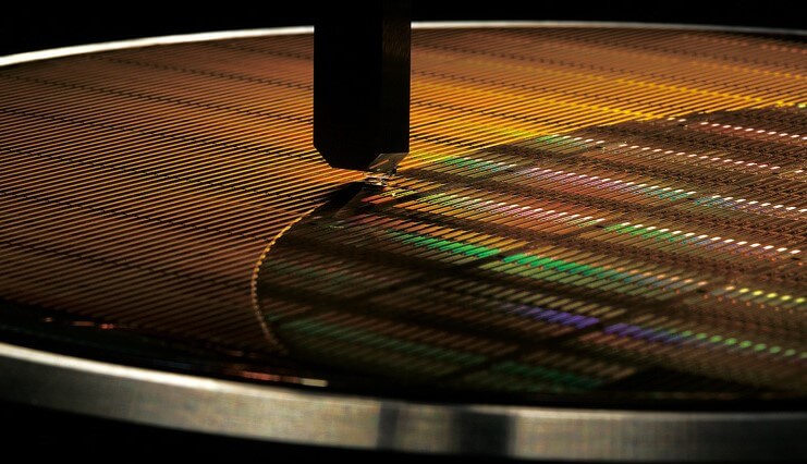
The process of dicing silicon wafers is critical for many device manufacturers. The process allows them to harvest many individual dices from a single wafer. The process requires high-precision machinery and skilled operators. The process of dicing semiconductor wafers is growing exponentially. If you have an existing manufacturing facility and want to expand into the semiconductor industry, consider using a stealth dicing system.
Another technique used for dicing wafers is scribe cutting. This technique uses a diamond blade to cut along the crystal plane of a wafer. The scribe cuts the wafer along the scribed lines and adds minimal residual stress to the chip. Additionally, there are no cooling requirements for scribe cutting. These features make stealth dicing wafers a better choice for many applications.
Traditional blade dicing
The traditional blade dicing process has several advantages. The dicing blade is versatile and can cut a variety of materials, including glass on silicon. The thickness of the blade used depends on the material and the amount of exposure it will have to the material. There are three main types of dicing blades. Each of these is useful for specific types of cutting. Choosing the correct dicing blade for a specific application is vital.
The blade bond hardness is the key to effective dicing. Harder materials require blades with a higher bond hardness, while softer materials require softer ones. The blade bond hardness is determined by the material’s hardness, and there are different scales for this. Generally, harder materials require a softer bond matrix, which limits its ability to be used in the dicing.
Another method for dicing wafers is scribe cutting. This method utilizes a diamond-like tool to cut the material. A diamond-like blade moves across the crystal plane surface of the wafer, applying pressure on the backside of the wafer and breaking it along the scribe lines. While both processes can produce similar results, scribe cutting is more efficient for certain applications because it adds no residual stress and generates no heat. It does not require coolants.
While conventional blade dicing is still an important process, there are better alternatives to it. Dry plasma etching can overcome some of the disadvantages of blade cutting, including chipping and cracking the die. Another dry plasma dicing process is Deep Reactive Ion Etching, which can etch narrow vertical trenches into the silicon and separate individual die. Besides, plasma dicing can be performed before or after grinding.
The cutting depth of a dicing blade affects the maximum spindle current. A higher feed speed reduces the radial wear of the dicing blade. However, a higher feed speed produces more heat, which melts the dicing blade quickly. These factors must be considered carefully when determining which dicing method is best for your specific requirements. If you are looking for a high-quality dicing process, make sure that you check the material’s properties before making a decision.
Laser ablation dicing
There are many advantages to laser ablation dicing. For one, it is noncontact and gentler than mechanical dicing. Unlike mechanical dicing, laser ablation starts at the top of the wafer and removes material layer by layer. This process is called “cold ablation” because the laser pulses have a short duration and do not transfer any heat to the atoms adjacent to the silicon. Laser ablation can damage delicate layers and devices, but the high speed is less likely to cause them to break.
The laser beam 16 has certain parameters that must be met to avoid ablation of the substrate wafer 28. At least one wavelength in this wavelength range must be set in order to ablate the silicon wafer. This will prevent damage to the substrate wafer. It will also create a patterned cut edge. A typical process is a combination of laser cutting and dicing. The combination of the two methods can reduce defects and process costs.
Laser dicing also uses high concentrations of photon streams to create a localized high temperature. By focusing the beam, the laser heats the material within the dicing lane, creating voids. When the water expands, the weakened regions tear apart. This process can be used to improve the quality of semiconductor manufacturing. But the process can cause problems for some devices. Therefore, it is recommended to test all processes before deciding on the right one for your process.
Moreover, laser ablation is expensive, which makes it uneconomical for many applications. A typical 500um silicon wafer will require a 20um term, which is equivalent to fourteen inches between two three-story buildings. A ball in such a small gap is nearly impossible to throw. Even if ultra-short pulsed lasers can remove the material, they are often very expensive.
The main advantages of laser dicing are the ability to handle thin wafers, reduced tool wear and material loss, and maximum machining speed. Laser dicing is a preferred dicing technology for thin wafers because it has the advantage of avoiding flaking at the cutting edges. Edge quality is one of the deciding factors in fracture resistance. Automated postprocessing improves edge quality and reduces production waste.
Cutting with a diamond blade
In semiconductor manufacturing, cutting with a diamond blade is used to separate dies from each other. The thickness and type of diamond particle/abrasive that a cutting tool has will determine the amount of exposure and the size of the blade. Also, the feed rate, spindle speed, and blade dressing will affect the results. Here’s a look at some of the benefits and disadvantages of cutting with a diamond blade for wafer dicing.
Dicing is a cutting process used to cut very hard and brittle materials. The resulting edge is nearly perfect. Dicing can be faster than sawing and does not require cooling water or residual stress. Dicing can be used to separate a die from a wafer. Some users dice a wafer into smaller pieces before reusing it. The materials for wafer dicing vary widely.
When selecting a diamond blade for wafer Dic, two factors must be considered: the speed of the process and the quality of the surface finish. The operator must find a balance between speed and blade life. Diamonds have a higher impact strength than the materials they cut. Impact ruptures the material, transferring momentum and electrical power from the cutting machine to break it apart. When cutting a semiconductor wafer, a high-quality diamond is an ideal choice.
The RPM of a dicing saw must be between 10,000 and 40,000 RPM. The right spindle speed must balance the two disadvantages of dicing with a diamond blade. A lower speed reduces the risk of the diamond breaking, while a high speed may cause the blade to fall out. However, the increased cost may offset the cost savings in consumables. If these are the two primary disadvantages of dicing with a diamond blade, they may not be worth the extra cost.
While a single nozzle can satisfy the directional requirement, it will fail to create intimate contact with the diamond blade along the sides. The result is a lower cutting efficiency and higher edge chipping damage, especially when processing brittle materials. Additionally, it may reduce the life of the diamond blade by causing erosion on the sides of the blade. Also, uneven cuts are common. If you’re using a dicing tool for wafer dicing, choose one with dual streams of coolant.